Semiconductors (Back-end)
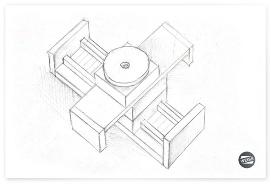
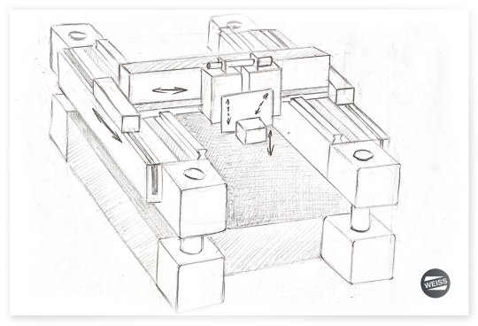
Customized Systems for High-tech Production
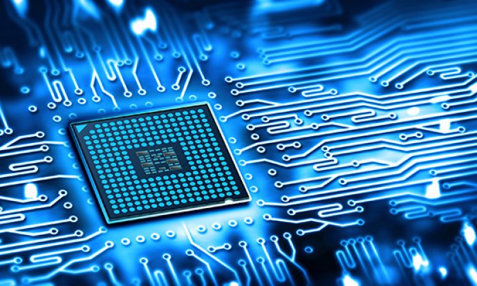
5G, autonomous driving, and AI are the driving forces behind new applications for networking machines and devices – applications that will continue to change our lives. Memory chips have a significant impact in this context and are included in all chains of action. High-performance microelectronics is a key technology for success in international competition. The production of semiconductors therefore brings with it particular requirements for the automation components: they must be absolutely vibration-free, with high speeds and positioning accuracy in the nano-range. This is another area where WEISS can provide customized multi-axis system solutions for many processes, ranging from dicing and die bonding to assembly.
Typical Processes
- Wafer dicing with XY systems
- Wafer inspection
- Die bonding
- Wafer-level packaging based on our gantry systems
Welcome to myWeissWorld
The individual access to the digital world of WEISS.