Wafer Probing
Tasks
The optical circuits arranged on the SiPh (Silicon Photonics) wafer must also be tested in many cases. For this purpose a centrally arranged XY-table is used to transport the wafer. Although the test tool also has several degrees of freedom in many cases, it is not able to cover the complete wafer surface.
Solution
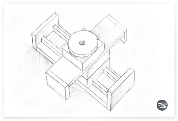
A customer-specific XY system is used around which several test stations can be arranged to increase throughput. Rough positioning is done by the XY table, fine positioning is done in several 6DoF alignment systems.
Benefits
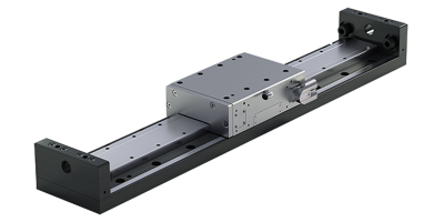
- Standard axes for Pick&Place tasks
- Customized solutions in all accuracy classes
- Development and production of the XY-table with the complete base
- The integrated high-resolution measurement system allows a high stability in position, with a jitter of a few nm
Photonics
Contact Person
Sachin Channe
Manager – Application Engineering & Segment Business develop
Phone +91 7030 844 413
sachin.channe@weiss-world.com
Products
Welcome to myWeissWorld
The individual access to the digital world of WEISS.
Use the CAD product configurator to configure rotary indexing tables, linear motor axes and pick & place modules according to your requirements.
Download generated or already preconfigured CAD models free of charge incl. matching technical documentation.
Once created, product configurations can be retrieved at any time from your personal account.
Stay up to date and receive news, product updates, trade fairs and dates as a newsletter.
Quick contact with a WEISS service partner.